


QR код

Продукти
Свържете се с нас


факс
+86-579-87223657

Електронна поща

Адрес
Wangda Road, Ziyang Street, Wuyi County, Jinhua City, Zhejiang Province, Китай


Vetek Semiconductor е водещ производител на пореста SIC керамика за полупроводниковата индустрия. Преминал ISO9001, полупроводник Vetek има добър контрол върху качеството. Vetek Semiconductor винаги се е ангажирал да стане новатор и лидер в порестата SIC керамична индустрия.

Пореста sic керамичен диск
Порестата SIC керамика е керамичен материал, който се изстрелва при високи температури и има голям брой взаимосвързани или затворени пори вътре. Известен е още като микропореста вакуумна чаша, като размерите на порите варират от 2 до 100.
Порестата SIC керамика е широко използвана в металургията, химическата промишленост, опазването на околната среда, биологията, полупроводниците и други области. Порестата SIC керамика може да се приготви чрез метод на пенообразуване, метод на SOL гел, метод за леене на лента, метод на твърдо синтероване и метод на пиролиза на импрегниране.

Подготовка на пореста SIC керамика чрез метод на синтероване
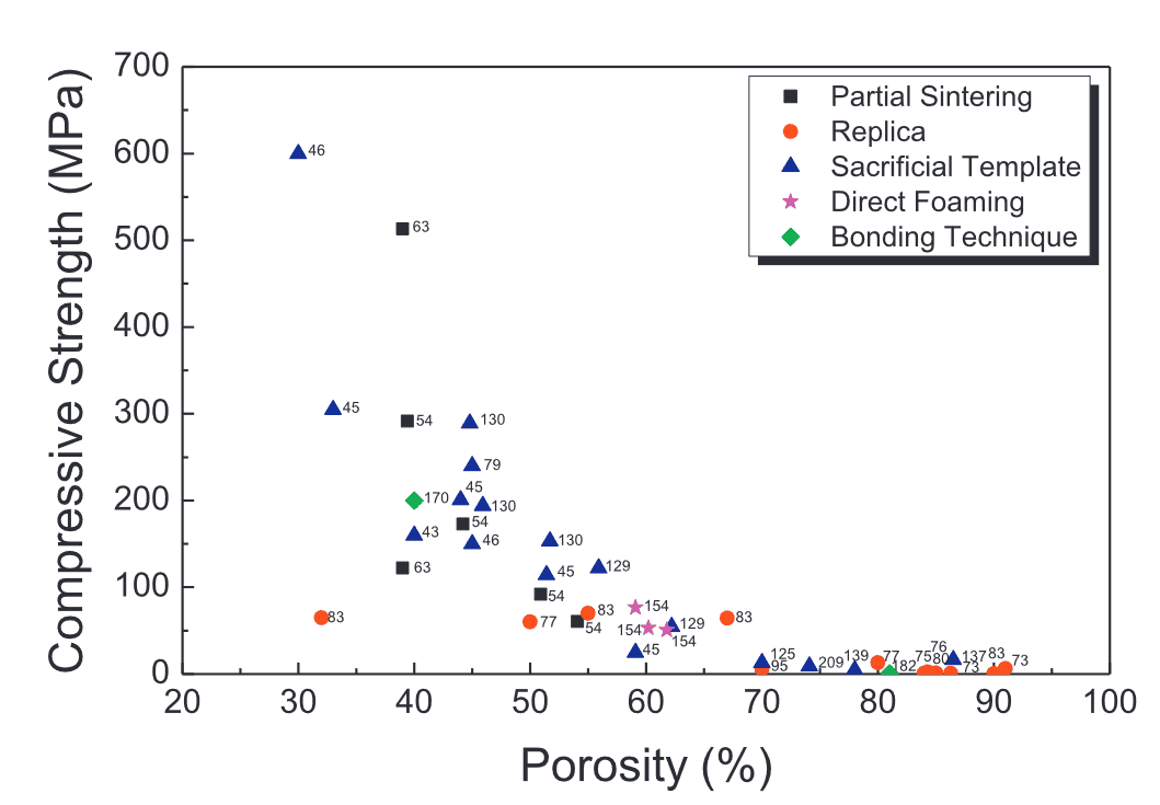
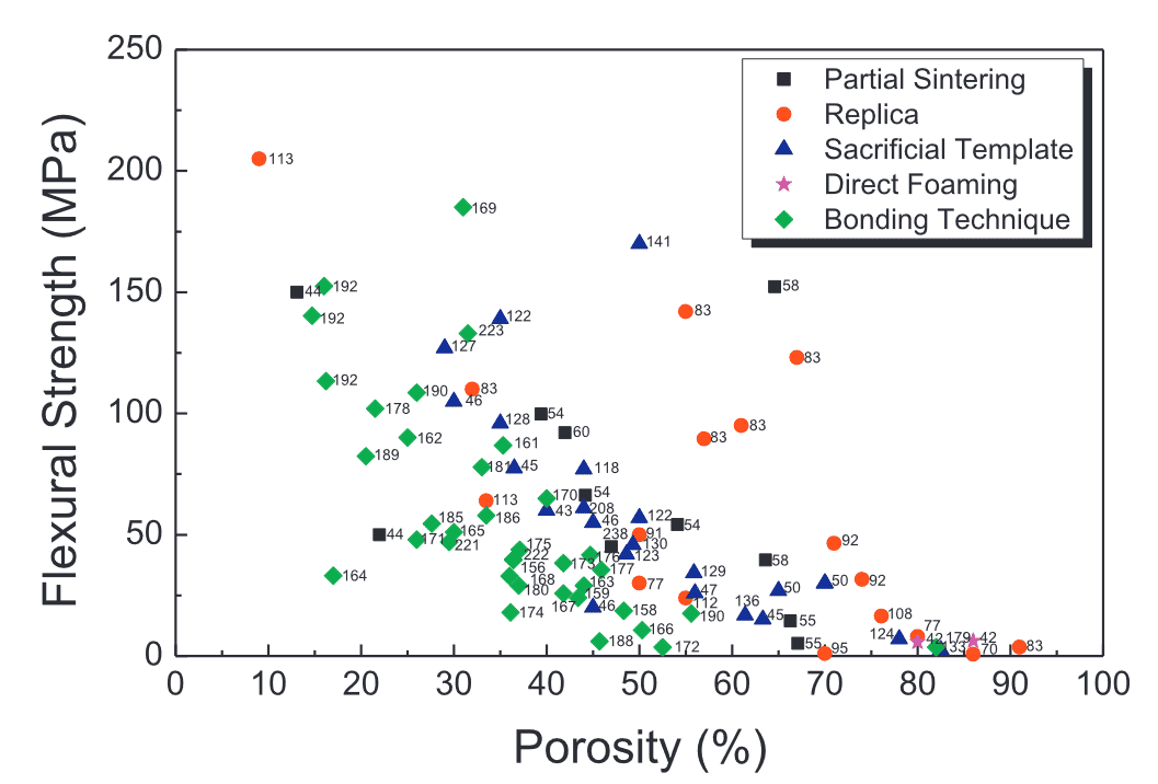
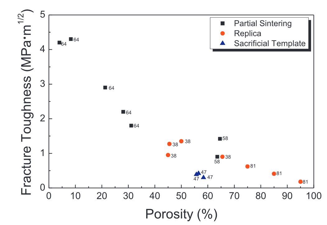
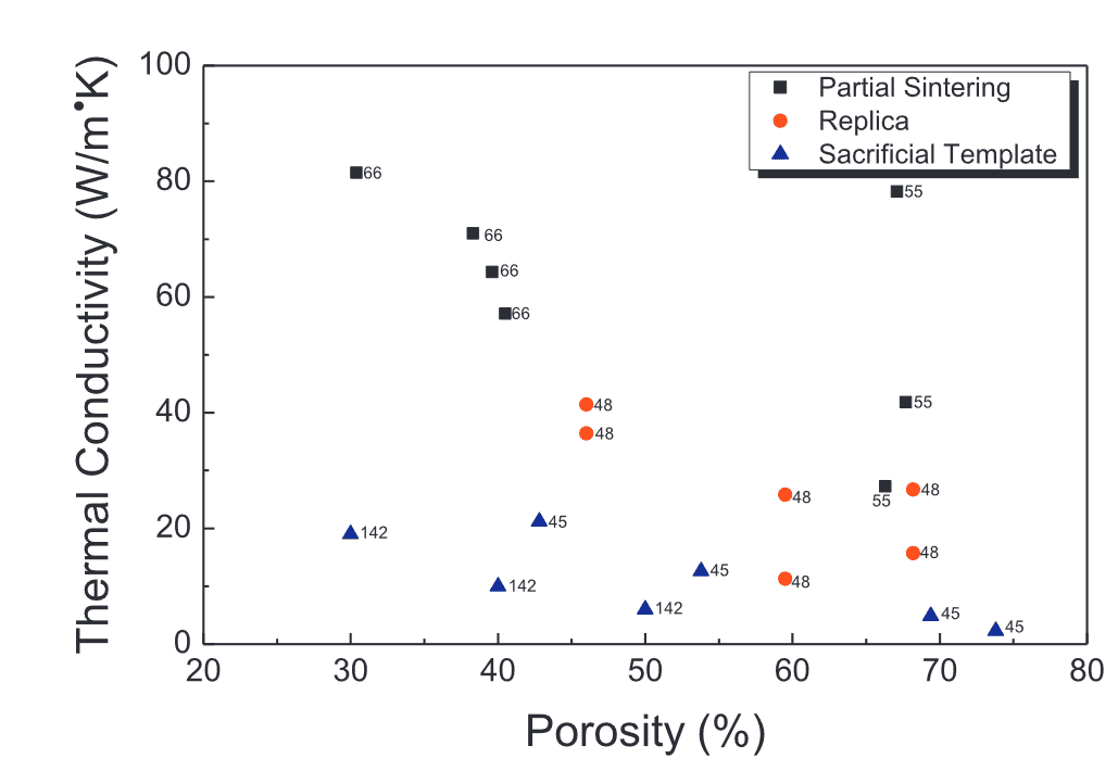
Свойства на пореста силициева карбидна керамика, приготвена по различни методи като функция на порьозността

Порести SIC керамика засмукване в производство на полупроводникови вафли
Порестата SIC керамика на Vetek Semiconductor играе ролята на затягане и носене на вафли в производството на полупроводници. Те са плътни и равномерни, с висока здравина, добри във въздуха пропускливост и равномерни при адсорбция.
Те ефективно се справят с много трудни проблеми като вдлъбнатини на вафли и разграждане на електростатични чипове и спомагат за постигането на обработката на изключително висококачествени вафли.
Работна диаграма на пореста SIC керамика:

Принцип на работа на порестата SIC керамика: Силиконовата вафла се фиксира от принципа на вакуумната адсорбция. По време на обработката, малките дупки на порестата SIC керамика се използват за извличане на въздуха между силициевата вафла и керамичната повърхност, така че силиконовата вафла и керамичната повърхност да са с ниско налягане, като по този начин фиксират силиконовата вафла.
След обработката плазмената вода изтича от дупките, за да се предотврати прилепването на силициевата вафла към керамичната повърхност и в същото време се почиства силиконовата вафла и керамичната повърхност.

Микроструктура на порестата SIC керамика
Маркирайте предимствата и функциите:
● Високотемпературна съпротивление
● Устойчивост на износване
● Химическа устойчивост
● Висока механична якост
● Лесен за регенериране
● Отлична устойчивост на термичен удар
артикул
единица
Пореста SIC керамика
Диаметър на порите
един
10 ~ 30
Плътност
g / cm3
1.2 ~ 1.3
Повърхностна ругаhness
един
2.5 ~ 3
Стойност на абсорбцията на въздуха
KPA
-45
Сила на гъвкавост
MPA
30 Диелектрична константа
1MHz
33 Топлинна проводимост
W/(m · k)
60 ~ 70
Има няколко високи изисквания за порестата SIC керамика:
1. Силна вакуумна адсорбция
2. Плодността е много важна, иначе ще има проблеми по време на работа
3. Без деформация и без метални примеси
Следователно стойността на абсорбцията на въздуха на порестата керамика на полупроводника на Vetek достига -45kpa. В същото време те се темперират на 1200 ℃ за 1,5 часа, преди да напуснат фабриката, за да премахнат примесите и да се опаковат във вакуумни торбички.
Порестата SIC керамика се използва широко в технологията за обработка на вафли, трансфер и други връзки. Те са постигнали големи постижения в свързването, дигирането, монтажа, полирането и други връзки.


Order precision-engineered Porous SiC ceramics from Veteksemicon—ideal for thermal uniformity and gas control in semiconductor systems.
Veteksemicon’s porous silicon carbide (SiC) components are engineered for high-temperature plasma processes and advanced gas flow control. Ideal for PECVD, ALD, vacuum chucks, and gas distribution plates (showerheads), these components offer excellent thermal conductivity, thermal shock resistance, and chemical stability.
Our porous SiC features a controlled pore structure for consistent gas permeability and uniform temperature distribution, reducing defect rates and enhancing yield. It is widely used in wafer handling platforms, temperature equalizing plates, and vacuum holding systems. The material ensures mechanical durability under corrosive and high-load thermal conditions.
Contact Veteksemicon today to request custom Porous SiC solutions or detailed engineering parameters.
+86-579-87223657
Wangda Road, Ziyang Street, Wuyi County, Jinhua City, Zhejiang Province, Китай